
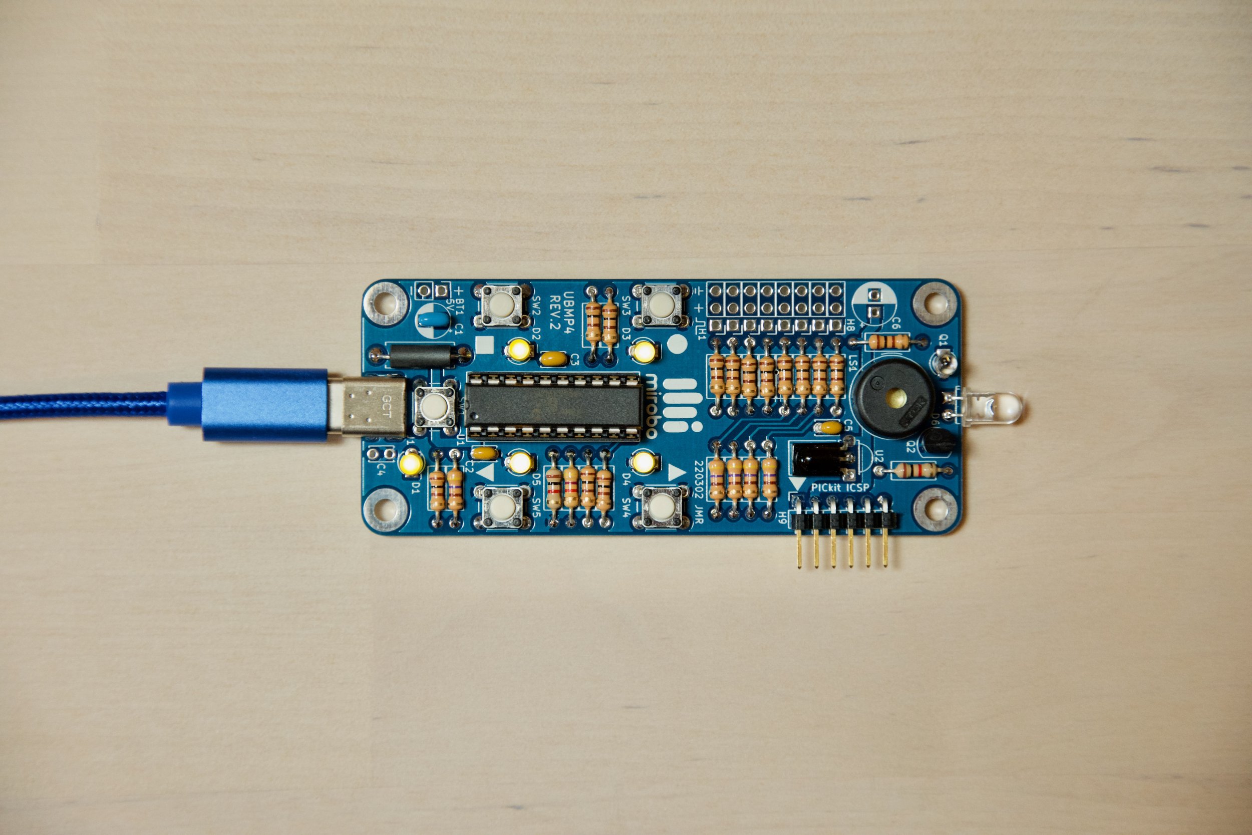
UBMP4 Introductory Programming Activity 5
Analog Input
Microcontrollers are primarily digital devices operating in our analog world of varying temperature, light levels, position, and other changing quantities. The PIC16F1459 microcontroller used in UBMP4 contains an analog-to-digital converter (ADC) specifically designed to measure analog quantities, allowing these inputs to be converted into digital numbers and processed by our programs.
The configuration and use of the ADC in the PIC16F1459 is reasonably complex, and the only way to really develop a full understanding of it is by referring to the ADC section of Microchip’s PIC16F1459 data sheet. Fortunately, a full understanding of the ADC is not required for simple conversions, and it can be used without too much difficulty with the functions included in the UBMP420.c file.
ADC hardware
Before using the ADC though, it is important to have at least a basic understanding of typical analog-to-digital conversion hardware and the conversion process. Let’s start with the analog input, work our way through the ADC hardware, and finish with the process of conversion.
Analog inputs
The PIC16F1459 microcontroller’s I/O pins are typically configured as either inputs or outputs. To use the analog-to-digital converter, the pins need to be set as another option – analog input. The TRIS and ANSEL registers, described in the first Introductory programming activity, can be configured to enable this.
What analog inputs are available for use? The PIC16F1459 microcontroller has a built-in temperature indicator module (TIM) that can be used as an input, and UBMP4 can be configured with an ambient light sensor or phototransistor soldered in as Q1 to sense analog light levels. External analog circuits can also be connected to some of the header pins, so a variety of input options are available.
Input reference
In simple terms, the ADC converts the voltage on a pin to a digital number. By default, the analog voltage has to be in the range between zero volts and the power supply voltage, usually 5V. Different reference voltages can be supplied to most ADCs to reduce the input voltage range and improve the accuracy of the output number, but the UBMP4 is designed to just use the default power supply references, 0V and 5V, to set the input voltage range.
Input multiplexer
The ADC is able to read the voltage from multiple microcontroller input pins and analog sources, but since there is only one ADC on the chip it can only do so from one input at a time. Before conversion, a multi-input analog switch, called a multiplexer (or, often shortened as mux.) is used to select the input channel to be sampled by the ADC.
After switching input channels, the analog voltage needs to charge the internal capacitance of the ADC circuit, essentially making its voltage the same as the voltage on the external input circuit. The time taken to stabilize the internal ADC voltage depends on the impedance (resistance) of the attached input circuitry, and how different the new input voltage is from the previously-converted voltage level. The higher the impedance, or the more different the new potential is, the more time should be given for the internal ADC voltage to stabilize before conversion. Since this capacitive effect is small, the delay time is typically just a few microseconds, but since microcontrollers are so fast it is important to account for this delay to get accurate and repeatable results when using the ADC.
SAR logic
The PIC16F1459 uses a successive approximation register (SAR) type analog-to-digital converter to save circuitry and power at the expense of conversion speed. A SAR converter successively guesses the output digital number using a binary search function. The SAR output is coupled through a digital-to-analog converter (DAC) and fed into a comparator with the input analog signal to both drive the SAR logic and home in on the final result.
Here is how it works. Imagine you and I playing a guessing game. I am thinking of a number between 0 and 100, and you have to guess my number. The number can be guessed in 7 guesses or less by successively dividing the search range down into halves. No matter what my chosen number is, your starting guess should be 50. If my chosen number is 32, I would let you know that it is lower than your initial guess. Your next guess would then optimally be 25, for which I would let you know that my number is higher than the second guess. Using this simple logic and an understanding of binary possibilities, we can know how many guesses are required for varying output possibilities – essentially, one guess per bit. So, guessing any number between 0 and 100 will take you just seven guesses. Obtaining an 8-bit result, or a number between 0 and 255, will take exactly 8 guesses.
The SAR in the ADC of the PIC16F1459 is a 10-bit converter, so it always takes ten guesses and provide an output result of between 0 and 1023. Each guess takes a short amount of time, and the input voltage should be stable for the whole conversion time taken by the ten guesses.
One last thing – even though the ADC completes a 10-bit conversion, the microcontroller provides the option to use only eight bits of the result. Why eight bits? If the extra precision isn’t needed, an 8-bit result is more convenient for an 8-bit processor, allowing for faster processing and smaller code than declining with a 10-bit result – which is often a worthwhile trade-off. The ADC functions that are part of the UBMP420.c code are designed to help you get started in your microcontroller journey and use the converter in 8-bit mode.
ADC clock
The SAR needs ten guesses to complete its conversion, and the conversion time should be as fast as possible for the best accuracy, but can’t go too fast either. What clock speed does it run at? Should the ADC clock be tied to the microcontroller’s clock?
For flexibility, the ADC and microcontroller can have separate clocks, or the ADC can use a divided-down microcontroller clock rate. The ADC clock has an ideal range, and that range is below the faster microcontroller clock options, so it may not match the chosen clock rate. In any event, your program needs to choose a clock source and clock frequency have to be chosen for the converter to use in performing a conversion.
ADC software and conversion process
Before an analog conversion can take place, these steps must be completed:
Analog input pin configuration
Voltage reference selection
ADC conversion clock selection
Input source selection
The ADC_config( ) function in the UBMP420.c file takes care of these steps for us. (There are additional functions in the UBMP420.c code to select and input channel, perform a conversion, or to select and then convert from an input channel.)
Once the ADC is configured and the input is selected, the analog conversion can start. Conversion is started by setting the GO bit in one of the internal ADC control registers. Since the ADC is a hardware module, it will complete the conversion entirely on its own and then clear the GO bit when the conversion is finished. Our program can choose to wait for the conversion to finish, or, alternatively, start the converter and then continue with other processing while the converter is running and grab its result later.
New Concepts
While computers are digital, the world they inhabit is analog. Here are some concepts that will be important to know:
ADC (Analog-to-Digital Converter) - divides the range between two different reference voltages into equal-sized steps, and outputs the digital code representing the input voltage
DAC (Digital-to-Analog Converter) - produces an output analog voltage representing the value of the numeric digital input
Comparator - a two-input analog amplifier that outputs the binary difference between an input and a reference voltage and produces a 0 output when the input is lower than the reference, and a 1 output when the input is higher than the reference
SAR (Successive Approximation Register) - a hardware counter circuit that, when combined with a DAC and comparator, forms part of a simple ADC by repeatedly guessing the input (taking 1 guess per bit of digital data)
Mux. (Multiplexer) - a multiple-input, single-output switch, commonly used to select one analog input out of many to feed into an ADC for conersion
LSB (Least Significant Bit) - the lowest value bit of a digital number, representing a value of 1
MSB (Most Significant Bit) - the highest value bit of a digital number
Serial data - the process of transmitting one bit at a time down a single wire by sending all of the data bits sequentially, either LSB-first, or MSB-first
Data output
After an analog conversion finishes, our program can read the result from the ADRESH register (or both the ADRESH and ADRESL registers for a 10-bit result). Since this example code configures the converter for an 8-bit result, ADRESH will contain a number between 0-255 (representing input voltages between 0V and 5V) that we can copy to any RAM variable. But, how will we know what the number is? UMBP4 has no display, no monitor connection, and only 5 LEDs. We could just do a simple comparison, lighting an LED if the analog value is above or below a threshold. But, without even knowing what number to expect, or even the approximate range of numbers, we won’t even know what to set the threshold value as.
The first method we will use to output the analog value is to send its result, 4 bits at a time, to the LEDs. Another option that can be used is to write the value to the header pins and read the state of each of the pins using a voltmeter. Both of these are a bit tedious, so this activity will also demonstrate another method you might be able to experiment with – serial output.
Serial output
Serial output can provide a more versatile option for debugging, but you will also need an oscilloscope, a logic analyzer, or a serial terminal see the results. An oscilloscope is the most commonly available of these tools in many electronics labs, and it will be the only option explored here. Any kind of oscilloscope will work, though a digital oscilloscope with a pulse-based trigger will make it easier to see the serial data. Many newer digital oscilloscope models have built-in serial decoding functions, making them very versatile debugging tools. Of course, if you have a logic analyzer or serial terminal available, you can try serial debugging with those tools as well.
The main program
This program builds on the concepts of functions introduced in the previous activity, using a new function in the main program, the analog functions found in the UBMP420.c file, and an example serial output function located in another source code file. Download the Intro-5-Analog-Input program files (.zip) to create the MPLAB project for this activity, or import the files into MPLAB from its Github repository. We will examine the contents of the main file, Intro-5-Analog-Input.c first:
/*==============================================================================
 Project: Intro-5-Analog-Input          Activity: mirobo.tech/ubmp4-intro-5
 Date:    May 9, 2023

 This introductory programming activity for the mirobo.tech UBMP4 demonstrates
 analog input, number base conversion, and the use of a simple, external serial
 output function library. (Serial output is a useful technique for debugging
 using a logic analyzer, or digital oscilloscope with a serial decode function.)

 Additional program analysis activities investigate the analog constants and
 input functions in the UBMP420.h and UBMP420.c files, as well as explore
 bit-wise AND operations for selectively clearing and testing bits.
==============================================================================*/

#include    "xc.h"              // Microchip XC8 compiler include file
#include    "stdint.h"          // Include integer definitions
#include    "stdbool.h"         // Include Boolean (true/false) definitions

#include    "UBMP420.h"         // Include UBMP4.2 constants and functions
#include    "Simple-Serial.h"   // Include simple serial functions

// TODO Set linker ROM ranges to 'default,-0-7FF' under "Memory model" pull-down.
// TODO Set linker code offset to '800' under "Additional options" pull-down.

// ASCII character code definitions
#define LF      10              // ASCII line feed character code
#define CR      13              // ASCII carriage return character code

// Program variable definitions
unsigned char rawADC;           // Raw ADC conversion result

// Decimal character variables used by binary to decimal conversion function
unsigned char dec0;             // Decimal digit 0 - ones digit
unsigned char dec1;             // Decimal digit 1 - tens digit
unsigned char dec2;             // Decimal digit 2 - hundreds digit

// Convert an 8-bit binary number to 3 decimal digits
void bin_to_dec(unsigned char bin)
{
    dec0 = bin;             // Store number in ones digit
    dec1 = 0;               // Clear tens digit
    dec2 = 0;               // Clear hundreds digit

    // Count hundreds digits in dec2 variable
    while(dec0 >= 100)
    {
        dec2 ++;
        dec0 = dec0 - 100;
    }
    // Count tens digits in dec1 variable, dec0 will contain remaining ones
    while(dec0 >= 10)
    {
        dec1 ++;
        dec0 = dec0 - 10;
    }
}

int main(void)
{
    // Set up ports and ADC
    OSC_config();               // Configure oscillator for 48 MHz
    UBMP4_config();             // Configure I/O ports for on-board devices
    ADC_config();               // Configure ADC and enable input on Q1
    H1_serial_config();         // Prepare for serial output on H1

    // Enable PORTC output except for phototransistor Q1 and IR receiver U2 pins
    TRISC = 0b00001100;

    // If Q1 and U2 are not installed, all PORTC outputs can be enabled by
    // uncommenting the line below:
    // TRISC = 0b00000000;

    // Enable on-die temperature sensor and set high operating Vdd range
    FVRCON = FVRCON | 0b00110000;

    // Select the on-die temperature indicator module as ADC input and wait
    // for the recommended acquisition time before A-D conversion
    ADC_select_channel(ANTIM);
    __delay_us(200);

    // Select Q1 phototransistor as ADC input (can be selected if Q1 is installed)
    // ADC_select_channel(ANQ1);

    while(1)
    {
        // Read selected ADC channel and display the analog result on the LEDs
        rawADC = ADC_read();
        LATC = rawADC;

        // Add serial write code from the program analysis activities here:

        __delay_ms(100);

        // Activate bootloader if SW1 is pressed.
        if(SW1 == 0)
        {
            RESET();
        }
    }
}
Program Operation
The main( ) function begins with the typical oscillator and UBMP4 board configuration functions, exactly as seen in the earlier introductory activities. These configuration functions are followed by the first use of the ADC_config( ) function found in the UBMP420.c file, and a completely new H1_serial_config( ) function added as part of this project in the Simple-Serial.c file.
The ADC_config( ) function configures the PIC16F1459 microcontroller’s on-board ADC for use in UBMP4, sets the Q1 input pin as the default ADC input, configures the ADC voltage reference and conversion clock, and selects the 8-bit data output format. The H1_serial_config( ) function prepares the H1 header pin for serial data output. We will take a closer look at the details of both of these functions a bit later.
The next few lines of the main program set the header pins as outputs. Leave this code unchanged if Q1 and U2 are installed in your UBMP4, as enabling all of the digital outputs would conflict with the input pin functions required for Q1 and U2. You can safely uncomment the second TRISC statement (and, to demonstrate proper technique, comment out the first) to use all of the header pins for digital output if your UBMP4 does not have Q1 and U2 installed.
    // Enable PORTC output except for phototransistor Q1 and IR receiver U2
    TRISC = 0b00001100;

    // If Q1 and U2 are not installed, all PORTC outputs can be enabled instead
    // TRISC = 0b00000000;
The next section of the code sets the on-chip temperature sensor to operate in the high voltage range using operating information found in Microchip’s PIC16F1459 data sheet. The ADC_select_channel(ANTIM) function is used to switch the multiplexer to select the on-chip temperature indicator module (TIM) as the ADC input. After connecting with the temperature module, the data sheet recommends a 200 microsecond delay to allow the ADC potential to stabilize, so this delay has been added in the code.
The temperature module has the advantage of being available on-chip, but the chip package will prevent it from responding to temperature changes quickly. If your UBMP4 has Q1 installed, it will respond to light levels faster, so this is a better option for testing. Light sensing can be enabled by un-commenting the ADC_select_channel(ANQ1) line at the end of this block of code:
    // Enable on-die temperature sensor and set high operating Vdd range
    FVRCON = FVRCON | 0b00110000;

    // Select the on-die temperature indicator module as ADC input
    ADC_select_channel(ANTIM);
    // Wait the recommended acquisition time before A-D conversion
    __delay_us(200);

    // Select Q1 phototransistor as ADC input (can be enabled if Q1 is installed)
    // ADC_select_channel(ANQ1);
The above code shows examples of using two different analog inputs in the ADC_select_channel( ) function, ANTIM, and ANQ1. How would a new programmer, learning to use the analog functions for the first time know what functions are available, what parameters they require, and how to use them? One answer is code documentation. Documented code makes it easy to determine what functions do and how they work. Of course, you can always peruse the code to get an overview of the functions available in a program (and, hopefully, find some good documentation along the way).
All of the analog functions, along with the ANTIM and ANQ1 constants, are described and defined in this project’s UBMP420.h header file. The comments introducing the ADC_select_channel( ) function in the header file have been reproduced, below, along with the function’s prototype statement:
/**
 * Function: void ADC_select_channel(unsigned char channel)
 *
 * Enable ADC and switch ADC input mux to the channel specified by one of the
 * channel constants defined above.
 *
 * Example usage: ADC_select_channel(ANTIM);
 */
void ADC_select_channel(unsigned char);
The comments for this function indicate that it takes a single parameter representing the channel number. All of the channel numbers have been defined as constants above this section of the header file.
It’s always helpful for programmers to add documentation and comments to describe the operation of their code. Not only does good documentation benefit others, who may be seeing and using the code for the first time, but good documentation can also act as a reminder and reference for the programmers themselves. Comments can provide instructions for a function’s use, serve as a reference for constants and variables, describe specific parts or the operation of the the code, and provide insight into how something was done, or why it was implemented in a specific way.
The input-output loop
The main program loop repeatedly samples the analog input using the ADC_read( ) function and outputs the digital representation of the data to the expansion header connected to PORTC. The delay limits data updates to a 100 ms update rate, or 10 samples per second.
    while(1)
    {
        // Read selected ADC channel and display the analog result on the LEDs
        rawADC = ADC_read();
        LATC = rawADC;

        // Add serial write code from the program analysis activities here:

        __delay_ms(100);

        // Activate bootloader if SW1 is pressed.
        if(SW1 == 0)
        {
            RESET();
        }
    }
The upper four (or four most-significant) bits of PORTC are shared with the four LEDs along the long sides of the microcontroller. Running the program will display the first four bits of the binary output code on the LEDs. A multimeter can be used to probe the signal pins of the lower four bits of the output (the four least significant bits) unless Q1 and U2 are installed. If installed, their pins, on headers H3 and H4, will show the U2 and Q1 output levels instead instead of the microcontroller’s digital output levels.
With that in mind, the four LEDs can be used to show all eight bits of the digital output by displaying each nybble (four bits) in succession. Replace the single __delay_ms(100); statement in the code above with the following code:
        __delay_ms(1000);
        LATC = rawADC << 4;
        __delay_ms(1000);
        LATC = 0;
        __delay_ms(1000);
After displaying the first four bits on the LEDs and then waiting for one second (1000 ms), the LATC = rawADC << 4; bit shift operator will move all of the rawADC bits four positions to the left before writing them to LATC. This effectively moves the lowest four bits of data into the upper four bit positions, allowing them to be displayed on the LEDs. A second time delay leaves this new output pattern on the display for 1000 ms before blanking the display, then waiting another 1000 ms, and eventually starting the main loop again.
Since this program always uses the same input channel, the code in the main loop uses the ADC_read( ) function, which just restarts the analog conversion. If your program needs to switch between different analog inputs, the ADC_read_channel( ) function combines the channel selection and analog conversion operations in the same function to simplify your code.
The digital values representing an analog input will eventually be put to use in other parts of your program, but it is still important for you to have an idea of what the values are, or what range they are in. While this code reads an analog level, converts the level to a digital value, and then outputs the result to an I/O port, reading the result using LEDs or a multimeter is tedious. In the next section, we will learn more about the analog configuration function as well as learn to use serial data functions to write the data out to an oscilloscope or serial device. Before you go on, comment out the lines that were added to revert the code above back to the single __delay_ms(100); statement before the addition of the extra display code.
Learn more – program analysis activities
Analog configuration
While the ADC needs to be configured before use, the full extent of the analog configuration is based on the features and data types you will need in your program. The ADC_config( ) function included in the UBMP420.c code is provided as a starting point, and you should learn to customize the analog configuration for your specific projects and circuits. Let’s explore the ADC_config( ) function as set up for these introductory activities in UBMP4:
// Configure ADC for 8-bit conversion from on-board phototransistor Q1 (AN7).
void ADC_config(void)
{
    LATC = 0b00000000;          // Clear Port C latches before configuring PORTC

    // Enable analog input and disable digital output for each analog pin below:
    TRISCbits.TRISC3 = 1;       // Disable output driver (TRISx.bit = 1)
    ANSELC = 0b00001000;        // Enable Q1 analog input (ANSELx.bit = 1)

    // General ADC setup and configuration
    ADCON0 = 0b00011100;        // Set channel to AN7, leave A/D converter off
    ADCON1 = 0b01100000;        // Left justified result, FOSC/64 clock, +VDD ref
    ADCON2 = 0b00000000;        // Auto-conversion trigger disabled
}
The actions in the ADC_config( ) function are based on the suggested instructions and tips in Microchip’s PIC16F1459 datasheet. Clearing LATC in the first line is not specifically required for analog configuration (since this function switches some PORTC pins from digital outputs to analog inputs), but it is often very important to pre-set port pin logic levels to known states before changing the functions of port pins to outputs in order to prevent unwanted or accidental activation of output circuits.
Single-bit operators
Configuring a physical PIC16F1459 pin for analog input requires setting the pin as an input with with its digital input circuitry disabled. These steps are accomplished by the next two lines of code. The expression TRISCbits.TRISC3 = 1; sets pin 3 of PORTC to be an input (represented by making the TRISC bit 1, as opposed to 0 for output) using a bit operator. The format of this bit operator instruction lists the 8-bit memory register by name first (TRISCbits), followed by a dot, and then the specific bit name (TRSIC3, or bit 3 of TRISC).
The use of the bit operator is very important here, as it affects only a single bit within the TRISC register and leaves all of the other bits un-changed. Given that this code runs after the initial port configuration (done by the UBMP4_config( ) function), we may not know which of the other PORTC bits have been set as inputs or outputs and need to be careful not to change their function when reconfiguring one of the port pins as an analog input.
For comparison, using the register operation TRISC = 0b00001000; to set pin 3 of the TRISC register to 1 would have forced all of the other TRISC bits to 0 in the process. The default configuration of TRISC, using the statement TRISC = 0b00001111; in the UBMP4_config( ) function, configures the four least-significant TRISC bits as ones, and a follow-up TRISC register operation may un-do that.
Register operations are fine for the initial configuration of the TRISC bits, but single-bit operators are important for later modifications. A little bit later in this activity, another method of selectively changing a specific bit using a logical operator will be introduced.
After the necessary TRISC bit is configured to make the selected analog pin an input, the digital circuitry has to be disabled by setting the ANSEL (analog select) bit matching the input pin. Here the code blindly overwrites the register using the ANSELC = 0b00001000; instruction. Wait, is it ok to do this? Should a single-bit operator be used instead? While using a bit operator is preferable, in this case overwriting the register is perfectly safe to do since none of the PORTC pins were previously set as analog inputs during the UBMP4_config( ) operation.
The last part of the ADC_config( ) function sets up the analog to digital control registers, ADCON0, ADCON1, and ADCON2, the to select the input multiplexer channel, converter clock source, the voltage reference, and the conversion output format. All of these settings are based on information provided in the microcontroller’s datasheet.
Serial configuration
While the analog configuration function is a part of the same UBMP420.c file used by all of the introductory programs, serial configuration is handled by a new function located in the Simple-Serial.c file. Function prototypes for the serial functions are found in the Simple-Serial.h file which is included near the top of the program using an include statement.
The Simple-Serial functions are just that – simple serial functions used to demonstrate software-based serial output as well as some useful and interesting coding techniques. Implementing actual serial communication is handled much better in hardware than in software, using the PIC16F1459’s EUSART (Enhanced Universal Synchronous Asynchronous Receiver Transmitter) module, but UBMP4’s pushbuttons occupy the serial transmit and receive pins preventing the from being easily used on this board. But, that’s ok, as we can get a better understanding of how serial transmission works if we have to do it ourselves.
Bit-wise operators
Just as in the analog configuration above, the H1_serial_config( ) function also needs to modify a single bit in a register to prepare an I/O pin for its task. This time, a bit-wise logical AND operator will be used to clear a single bit in the TRISC register instead of using a single-bit operator instruction:
// Configure H1 for serial output and set output pin high for idle state
void H1_serial_config(void)
{
    TRISC = TRISC & 0b11111110;
    H1OUT = 1;
}
As we learned before, the TRISC register controls the data direction of the PORTC pins – 1 for input, and 0 for output. This program needs to make the H1 pin, or bit 0 of the register, a serial output, so its TRISC pin must be made zero. Again, without knowing the state of the other TRISC bits it would be unwise to overwrite the entire register. In this case, the logical AND operator ANDs each bit in the TRISC register with the constant 0b11111110. Any TRISC bits ANDed with 1 remain unchanged, and the lone TRISC bit ANDed with 0 is cleared.
The second line of code just sets the newly-configured H1 output pin high, which represents the idle state of the serial data line.
Asynchronous serial data transmission
Serial data bits are transmitted sequentially, one bit at a time, on a single conductor or data pin. Two serial data transmission methods are commonly used: asynchronous (self-clocked), and synchronous (clocked). Different bit encoding schemes can also be used, and one of the simplest and oldest commonly implemented serial transmission schemes commonly implemented in microcontroller hardware and software is the EIA RS-232 standard for asynchronous data transmission.
As a self-clocked standard, RS-232 serial data is limited to short sequences of bits to prevent timing drift errors between devices with independent clocks. RS-232 data is typically seven, eight, or nine bits long, transmitted between required (non-data) Start and Stop bits. The most common format is one Start bit, followed by eight data bits, and then one Stop bit, often shortened to 8N1 – where 8 represents the number of data bits, N means No parity bit has been added (even (E) and odd (O) are also allowed), and the final 1 represents a single Stop bit (1.5, and 2 Stop bits are also allowed).
Using 5V logic levels, the Start bit is low, or 0, and the Stop bit is high, or 1. The data is transmitted LSB-first (least-significant bit first), and the data line is left in the Stop bit’s state, also know as the idle state, until the start of the next transmission. Each bit is active for a time period equal to the reciprocal of the data bit rate. So, using a common data rate of 9600 bps (bits-per-second), the duration of each bit would be 1/9600s, or approximately 104 µs.
The yellow trace in the oscilloscope screen capture, below, shows the ten bits making up an 8N1-formatted data serial data stream transmitted at 9600 bps. The blue scale indicates the duration of each bit in the data frame. Note that this oscilloscope has a serial decoding function that decodes the transmission and displays all eight data bits, in their proper bit order, underneath the waveform:

Eight bits of RS-232 serial data transmitted LSB-first, with the decoded data in the proper bit order, below.
Serial write function
Now that we have an understanding of what serial data transmission is, we can explore the operation of the H1_serial_write( ) function included in the Simple-Serial.c file to see how it can be done. This function accepts one byte of data for transmission and runs at a fixed 9600 bps bit rate:
// Write one byte of 9600,8,N,1 serial data (9600 bps, 8 data bits, no parity, 1
// stop git) to H1
void H1_serial_write(unsigned char data)
{
    // Write the Start bit (0)
    H1OUT = 0;
    __delay_us(104);    // Delay for 1 bit time (equal to 1/9600 s)

    // Shift 8 data bits out LSB first
    for(unsigned char bits = 8; bits != 0; bits--)
    {
        if((data & 0b00000001) == 0)    // Check the least significant bit state
        {
            H1OUT = 0;
        }
        else
        {
            H1OUT = 1;
        }
        __delay_us(103);    // Shorter delay to account for 'for' loop overhead
        data = data >> 1;   // Prepare next bit by shifting data right 1 bit pos
    }

    // Finish the transmission by writing a Stop bit (1 - same as the idle state)
    H1OUT = 1;
    __delay_us(104);
}
Assuming that the H1 header pin was set as an output by the previous serial configuration code, the first two lines in this function create the Start bit by making the H1 output pin low and then waiting for one bit period of delay. Following the start bit, a loop was chosen as the most code efficient means of transmitting the eight data bits. The loop code used here combines two of the concepts seen earlier in this activity, namely bit-wise logical operators, and bit shifting.
Since RS-232 formatted serial data is transmitted LSB first (least-significant bit first), a method to extract the right-most bit, followed by the second bit from right, then the third from right, etc. is needed. The conditional if structure if((data & 0b00000001) == 0) does this for the right-most bit. It extracts the bit by isolating it using a bit-wise AND operator to clear the other seven bits, and compares the remaining data byte with 0. The if condition then outputs the matching 0 or 1 value to the header pin.
The bit output code is followed by a bit period delay that is slightly shorter (103µs vs. 104µs) to account for the time taken by the microcontroller to run the code that makes up the loop, including the conditional code within the loop. (The C language makes it easy to forget that a number of machine code instructions are used to create all of these structures, and each machine code instruction takes a small, but fixed amount of time to run.)
After the right-most bit of data has been sent, the second bit from right needs to be extracted from the data and transmitted. Instead of using eight different AND operators (one for each bit position in the data code), the data variable is itself shifted one bit to the right, moving its second bit into the position formerly occupied by the first bit. This allows the same conditional bit-wise operator already in the code to be re-used for each of the eight bits of data.
Repeating the process eight times, each of the data bits will be successively shifted into the LSB position to be read and transmitted on the H1 output pin. After all eight data bits have been sent, the last two lines of code add a Stop bit to finish the transmission and end the function.
It’s time to add this serial write function to the program. Modify your main program by adding the following line below the comment, as shown, to serially output the analog value:
        // Add serial write code from the program analysis activities here:
        H1_serial_write(rawADC);
If you have an oscilloscope, connect the probe to the H1 header data pin to view the serial data waveform. For oscilloscopes without a serial decoding option, set a falling-edge delay or pulse trigger to display each serial data transmission.
Serial data formatting
Serial data output can be a simple and versatile debugging option since it adds minimal extra program code and uses only a single I/O pin. (It can also be used as a method of chip-to-chip communication, but doing so is usually better implemented through the asynchronous or synchronous serial hardware modules built into microcontrollers.) Formatting the raw data with some additional characters may make it easier to read, or enable its use with serial terminals or displays. We will use this program’s internal bin_to_dec( ) function to format the data into individual decimal digits, and then demonstrate sending the data as multiple ASCII digits with extra formatting codes typically needed to display them on a multi-line serial display.
ASCII conversion
ASCII (American Standard Code for Information Interchange) is a commonly used code developed to encode Latin numbers and letters, punctuation symbols, and a variety of device control codes into 8-bit characters. Since ASCII is understood by most devices with serial decoding, we can use ASCII to display a decimal number representing an analog value instead of the binary digits. In the example oscilloscope capture above, the binary value 01111101 represents the number 125, and it can be decoded by the oscilloscope to display in decimal as 125 instead. We can also create our own software encoder to convert the data to ASCII, and then display the result as three separate ASCII digit characters: 1, 2, and 5.
The first step in converting our 8-bit data to ASCII is to convert the analog result variable into three variables representing the hundreds, tens, and ones digits. The bin_to_dec( ) function accomplishes the decoding using a simple algorithm to repeatedly subtract the digit weights of each digit from the original value until it can’t anymore, before attempting to do the same with the next digit. Add the bin_to_dec( ) function call to your program, along with the new serial write functions to output each of the decimal digits using the following code:
        // Add serial write code from the program analysis activities here:
        H1_serial_write(rawADC);

        // Convert ADC result to decimal and write each digit serially
        bin_to_dec(rawADC);
        H1_serial_write(dec2);     // Write each digit serially
        H1_serial_write(dec1);
        H1_serial_write(dec0);
The oscilloscope has been set to decode the serial data into decimal. The result, after running this code, will produce a serial output similar to the one shown below:

Four successive bytes of serial data showing the original value, and the individually decoded decimal digits.
The complete analog data has been transmitted first, followed by the data decoded into its constituent decimal digits. Each decimal digit is transmitted separately as its own binary number. The next step is to transform the binary digit codes into their equivalent ASCII character codes. For numbers, this is easily accomplished by adding 48, or as more commonly seen in programs, the equivalent hexadecimal code 30, shown in the program as 0x30. For output to a serial terminal, the program also shows the addition of the carriage return and line feed characters used to return the cursor to the beginning of a line and to add a new line.
        // Add serial write code from the program analysis activities here:
        H1_serial_write(rawADC);

        // Convert ADC result to decimal and write each digit serially in ASCII
        bin_to_dec(rawADC);
        H1_serial_write(dec2 + 0x30);   // Convert each digit to ASCII
        H1_serial_write(dec1 + 0x30);
        H1_serial_write(dec0 + 0x30);
        H1_serial_write(CR);            // Carriage return character
        H1_serial_write(LF);            // Line feed character
Running this program, with the oscilloscope set to decode ASCII provides the following output:

The ASCII codes representing the original value, the decoded and converted digits, and the CR and LF codes.
A serial terminal would display the ASCII characters for each code, and interpret the carriage return and line feed codes to move the cursor to the start of the next line. Running this program on a serial terminal would produce a new line of data for every value, once every 100 ms, like this:
}125
}125
}125
}125
}125
...
The } character represents ASCII code 125. Commenting out the original H1_serial_write(rawADC); statement added before ASCII decoding would remove the } character from the output, leaving only the ASCII digit codes and the carriage return and line feed control characters.
Activity 5 learning summary
Analog to digital converters (ADCs) allow the potential applied to an I/O pin to be read and converted to a numeric variable inside a microcontroller. Analog to digital conversion allows our programs to make decisions based on the magnitude of the analog value, or to use changing potentials from external circuitry as an input to our programs.
After analog conversion, determining the resulting analog value (or its range of possible values) can be a challenge if there is no easy way to output and read multiple bits of data. One solution is to output the data serially, though this requires the use of test equipment capable of displaying or decoding the serial values. The advantage though, is that serial output allows multiple bytes of data to be transmitted out of a microcontroller using just a single I/O pin.
Configuring microcontroller hardware devices as well as sending and receiving serial data often require the ability to modify or read individual bits within memory registers. There are bit operators in Microchip’s C language designed to control port pins, and bit-wise logical operators can be implemented in similar ways to isolate bits in any variable.
The PIC16F1459 contains a flexible ADC hardware module, a temperature sensor, asynchronous (EUSART) and synchronous (MSSP) modules for serial communication, and a variety of other hardware capabilities. Microchip’s PIC16F1459 data sheet provides the definitive reference information for all of these devices and should be consulted whenever implementing any of these features. The functions included for analog conversion, decimal decoding, and serial output in these introductory programming examples are designed to quickly help new learners gain a basic understanding of these processes and work well enough for many simple tasks. However, there are better ways to accomplish some of these things, and far more capabilities available through the hardware than have been described. We encourage you to keep learning and investigate these hardware features in the microcontroller’s datasheet.
Programming Activity 5 Challenges
1. The bin_to_dec() function converts a single byte into three decimal digits. Step 8 in the program analysis activities, above, converted each of these numeric digits to the ASCII code representing the digit. Can you make a bin_to_ASCII() function that would eliminate the need for you to offset the values to ASCII separately, as was done here?
2. Does your UBMP4 have Q1 installed? If installed, it will be easier to use Q1 as an input device instead of the temperature module. Q1 can either be an ambient light sensor, which is sensitive to visible light, or a phototransistor, sensitive to infrared (IR) wavelengths. Try using your phone's flashlight (ambient light sensor) or an infrared LED to illuminate Q1.
Create a program to implement threshold detection. Determine the analog level when Q1 senses low light and again when Q1 senses bright light. Use conditional code to light an LED when the Q1 light level rises or falls beyond a threshold set in your program.
3. Create a program that produces a PWM output proportional to an analog input, or a program that creates a tone having a pitch proportional to an analog input value.
4. If you have an oscilloscope available, investigate how fast you get the serial output to transmit. Try setting the bit delays inside the serial write function to 1 microsecond of delay, instead of 104 and 103. Does it work the way it should? Is each bit 1us long? What do you think is happening?
5. Creating a function to transmit serial data is relatively straight-forward. Receiving serial data reliably is similar, but should take into account slight timing differences between the transmitter and receiver. Think about how you would create a function to receive serial data. How could you ensure that the data is received correctly even if there are slight timing differences between the transmitting and receiving devices? Create the pseudocode or a flowchart describing a serial receive function.
6. Transmitting serial data involves isolating each bit of a variable to be sent using bit-wise logical operators, and bit-shifting the remaining data from within a loop. Received serial data can be assembled into an 8-bit variable using a similar technique. Try to create a function or just the main loop of code that would successively read serial data from an input pin and assemble the values into an 8-bit variable.